SiC semiconductors perform considerably well on various parameters like high temperatures, frequency, voltage, and several others.
In the industry associated with electronic instruments, the innovation in wide bandgap semiconductors has proved to be profitable and effective in comparison to traditional silicon-based semiconductors. Silicon Carbide (SiC) wide bandgap semiconductors are one of the most advanced semiconductors that offer prominent relevancy. These semiconductors perform considerably well on various parameters like high temperatures, frequency, voltage, and several others.
Through its mature manufacturing process, Silicon Carbide (SiC) has incomparable electrical properties that make it capable of being incorporated into next-generation device fabrication. The SiC-JFET is attracting the market towards itself due to its fast-switching speed and low on-state resistance, making it a high-demand material in the rising commercial market of the electronics industry.
A team of researchers affiliated with the University of Monastir in Tunisia and Université de Lyon in France, developed a multidimensional structure of the JFET to improve the performance and validate it through testing on the model [1] already presented in the paper, “A Multi-physics Model of the VJFET with a Lateral Channel” [2].
The Layout and Features of a JFET

A JFET is a unipolar device with two channels connected in series formation– the lateral channel and the vertical channel. Manufactured by SiCED/INFINION (TO220 package), the 1200V SiC JFET has a die size of 2.4×2.4mm2 and an on-resistance of 300mΩ with a threshold gate voltage of -20V and a saturation current of 20A.
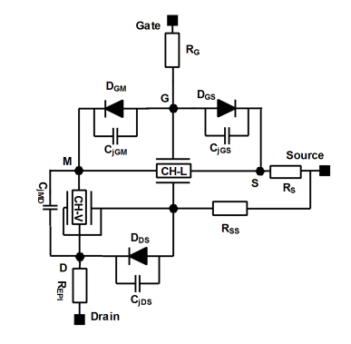
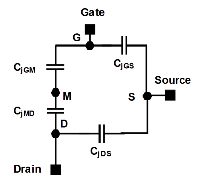
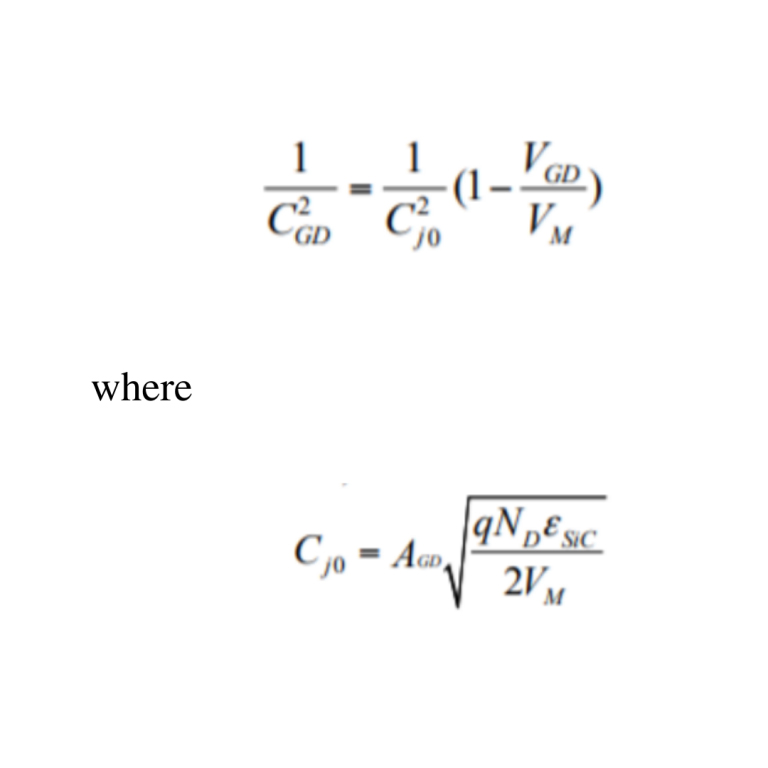
In the static and dynamic circuit model of JFET, we can see three physical capacitances: between gate and source (CjGS), gate and point M (CjGM), and drain and source (CjDS), with an additional capacitor between drain and point M (CjMD). To plot the C-V (Capacitance-Voltage) characteristics, the static and dynamic circuit model undergoes blocking conditions, which means there will be no static current flow in the channel. When the model is under prescribed conditions, the operating frequency is set to 300 kHz, which results in the impedance of the capacitors being greater than all the resistances present in the model circuit.
It is clear in the resultant circuit model shown in figure 3 that the capacitors will only affect the characteristics because the resistances are low in comparison to the capacitors. Taking the total capacitance between each terminal of the JFET, we get CGS, CDS, and CGD. [Note: Two capacitors between gate and drain are in series, hence they are taken as per the formula for resultant (total) capacitance between the two points.
CGS= CJGS
CDS = CjDS
1/CGD = 1/CjGM 1/CjMD
Numerical simulation
The researchers decided to use ISE TCAT Software for 2D numerical simulation of the SiC-JFET under predefined parameters, which are available in the research paper.
To start the simulation, a negative gate bias of -20 V is applied to make sure that the JFET is set to the off state. The capacitances can be extracted in the numerical simulations with a small AC signal analysis superimposed on the DC bias voltage when the lateral channel is completely blocked.
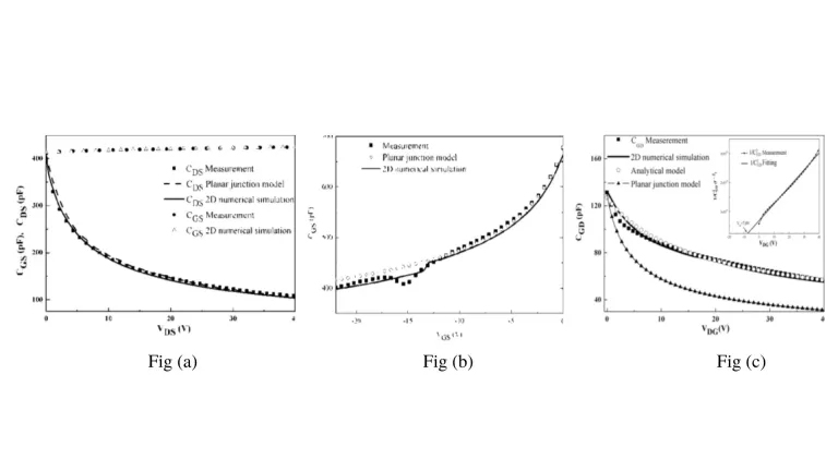
The below figure shows the comparison between CDS(VDS), CGD(VGD), CGS(VDS), and CGS(VGS) which are the measured characteristics, and those which are obtained from the 2D numerical simulations and analytical model.
Analysis of the numerical simulation
Following the numerical simulation, the results and measurements of the capacitances CGD, CGS, and CDS are analyzed, and the capacitance values are related to the associated space charge (SCR) width. The following criteria will be applied to the computation of SCR’s boundary.
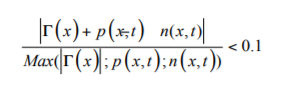
From the above equation, Г(x) is the net doping concentration, p(x,t) is the net hole concentration and n(x,t) is the electron concentration, where x and t are space and temporal variables, respectively.
The measured, numerical simulated, and analytical models of both planar junction gate-source CGS and CDS capacitances, versus VDS, respectively are presented in the simulated graphs. According to the equations for the model of CDS , it has been observed that CGS (spotted as a circle and top arrow around ~400pF capacitance) weakly increases with VDS but, CGS depends on VGS and is similar to a gate-source planar capacitance. The researchers noticed that the experimental and simulation results agree in this case, which is not true in the third case of CDS and CGS capacitance, where the CGD capacitance does not fit with a planar junction capacitance. To solve this discrepancy, based on TCAD numerical analysis, the team proposed an analytical model of the CGD capacitance.
Using the analytical model, it can be concluded that there is a correlation between the capacitance measured by CGD and the capacitance computed.
SiC JFET Dynamic Model Validation
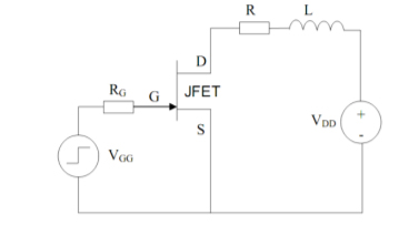
Validation of the proposed methodology is very important for any experiment. To do so, the team conducts tests to assess the validity of dynamic performances in switching situations. The load resistance R, load inductance L, and gate resistance RG are all part of the inductive switching simulation circuit.
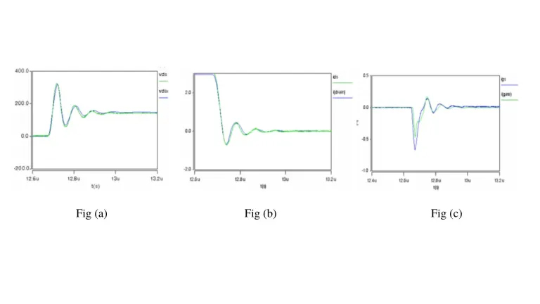
Looking at the comparison of simulation (blue waveforms) and experimental (green waveforms) results for inductive-resistive switching turn-off, we can see that both are in good agreement. for inductive-resistive switching turn-off, we see that both the results are in good agreement with each other. The points where both the waveforms coincide are ideal points. However, in a practical scenario, there will be some difference in error. The aim is to reduce the error to get optimized results.
Conclusion and Analysis
The research article is based on the work carried out in [2] aiming to improve and validate the multidimensional structure of the JFET. Under blocking conditions (static current = 0A), starting with the static and dynamic circuit model of the JFET resulted in capacitors in series and parallel between each terminal of the JFET. The numerical simulation for C-V characteristics demonstrated different results with a few results not following the same pattern as others. In this [1] research article, the team developed a dynamic model for the vertical SiC JFET with a lateral channel that takes the multi-function effect in the terminal capacitance into account. Later, the dynamic model was performed in VHDL-AMS software, where the simulation results were validated with experimental results under inductive-resistive switching conditions and under capacitance-voltage measurement.
The research paper is published in the Proceedings of the Fourth International Conference on Engineering & MIS 2018 under closed access.
References
[1] M. Hervé et al., “A multi-physics model of the VJFET with a lateral channel,” Proceedings of the 2011 14th European Conference on Power Electronics and Applications, 2011, pp. 1-10.
[2] Sami Ghedira, Hervé Morel, and Kamel Besbes. 2018. Dynamic Circuit Model of SiC VJFET For Power Integrated Circuit Design. In Proceedings of the Fourth International Conference on Engineering; MIS 2018 (ICEMIS ’18). Association for Computing Machinery, New York, NY, USA, Article 48, 1–6. DOI:https://doi.org/10.1145/3234698.3234746