In flyback converters, the choice of the MOSFET is critical for increasing efficiency and power density while reducing size and weight
Higher efficiency and increased power density are needed in LED drivers, chargers, and other applications based on flyback converters, to conserve energy and reduce equipment size and weight. The choice of the flyback MOSFET is critical. In particular, the latest improvements in device geometry and fabrication process, aimed at lowering the drain-source on-resistance (RDS(on)) x silicon area figure of merit (FoM), make a significant contribution towards meeting these requirements.
Flyback converter overview
For low- and medium-power applications, the flyback converter is the most widely used topology because of its relatively low system cost and ease of design. Although the flyback topology suffers from a slightly lower efficiency than other topologies, it is a very popular choice for AC line-powered applications due to the electrical isolation provided by the transformer. Another useful characteristic of the flyback topology is its ability to produce multiple output voltages on separate secondary windings of the same transformer. The main target applications for the flyback topology are chargers, adapters, and LED drivers from 10 W to 75 W. Figure 1 shows a simplified flyback converter block diagram.

The two common modes of operation for the flyback are fixed frequency (FF) and quasi resonant (QR) switching. The choice depends on many factors including power, efficiency, form factor, and development time. As the name suggests, FF flyback switches operate with a pre-defined fixed switching frequency. They can operate either in continuous conduction mode (CCM) or discontinuous conduction mode (DCM).
DCM Flyback (Fixed Frequency)
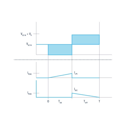
DCM flyback is typically used at low output loads. Its key advantage is that there are no reverse-recovery losses in the output rectifier. On the other hand, DCM flyback does have the disadvantage of very large ripple currents, which may require large EMI filters. The principle of operation and simplified waveforms are shown in Figure 2 below. Here during the turn-on phase of the flyback MOSFET (ton) the current builds up in the inductor to the peak value ILPK and when the MOSFET is turned off the current goes to zero before the MOSFET is turned on again.
CCM Flyback (Fixed Frequency)
A CCM flyback operates at fixed frequency and is typically used for adapters and small chargers in the higher power range, above 45 W. The advantages of operating in this mode are the small ripple and RMS currents, which result in lower I2R losses due to the equivalent series resistance (ESR) of the capacitor. Lower peak currents also allow smaller filter components.
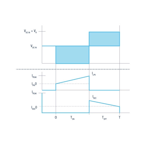
The most noted disadvantage of CCM flyback is the need for a higher inductance, which may require a larger magnetic component. Figure 3 shows the principle of operation and simplified waveforms. During the turn-on duration of the flyback MOSFET, the current starts rising from a non-zero value to a peak value ILPK in the transformer primary. During the turn-off of the MOSFET, the current starts decreasing but does not reach a zero value.
QR flyback (variable frequency)
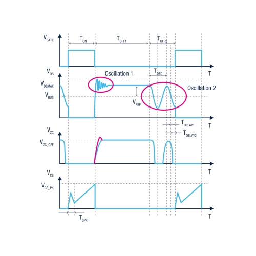
A quasi-resonant flyback is a DCM flyback that has a valley-switching turn on. It is largely used in low-power switched-mode power supply (SMPS) applications such as chargers, adapters, and auxiliary power supplies. The major benefit of a QR flyback is the lower turn-on loss of the MOSFET. In addition, conducted EMI is lower since the switching frequency is modulated, which effectively distributes the noise energy over a broad frequency spectrum. Despite these benefits, there are also some drawbacks. Since this is effectively still a DCM flyback, the peak and RMS current values remain higher as compared to CCM flyback. This will result in higher MOSFET conduction losses and increased losses in the transformer primary winding. For this reason, the QR flyback is not recommended for applications operating at higher power ratings or over a wide range from 65 W – 100 W and above. Figure 4 illustrates the principle of operation with simplified waveforms.
Power MOSFET Requirements for High Performance in Flyback Converters
Irrespective of which mode of operation is used for the flyback converter, the choice of the switch and its parameters significantly influences the overall performance. On one hand the flyback converter topology and its operation results in a high voltage stress on the switch, which places a higher breakdown-voltage requirement on the flyback switch when turned off. On the other hand, increasing the breakdown voltage of a FET adversely affects important figures of merit because of increased die size and higher input and output capacitances.
To overcome the challenges posed by market requirements, STs newly introduced MDmesh K6 technology offers compelling benefits in SMPS flyback topologies in adapters and chargers, LED lighting, smart metering, auxiliary power, and industrial power supplies.
MDmesh K6 technology, with a breakdown-voltage capability of 800 V, offers a lower RDS(on) simultaneously with reduced input and output capacitance. This leads to a more efficient switching at any given frequency combining high performance with high power densities. The 800 V class is the first to be released in this new family. ST plans to extend MDmesh K6 devices to other voltage classes in the future.
Important MOSFET device parameters to consider are the gate charge (Qg) and the energy stored in the output capacitance (Eoss) because they make a significant contribution to switching losses. Qg is closely linked to the effort needed to drive the MOSFET: smaller values lead to lower driving losses. Lower Eoss benefits hard-switching applications the most, as the energy stored in the output capacitor during the off state is dissipated in the MOSFET channel when the FET turns on. Reduction of this energy dissipated corresponds directly to energy saving and minimizing the overall power losses in the converter. Of course, the RDS(on) is also an important device parameter that determines conduction losses and has a critical role at higher power ratings.
Efficiency Performance of New 800 V MDmesh K6
The MDmesh K6 is the latest very-high-voltage super-junction (SJ) MOSFET technology from ST. The 800 V MDmesh K6 series is the successor to the MDmesh K5 series which is already established in the market. It combines the benefits of a fast-switching SJ MOSFET with excellent ease of use. Furthermore, extremely low switching losses make switching applications even more efficient and compact.
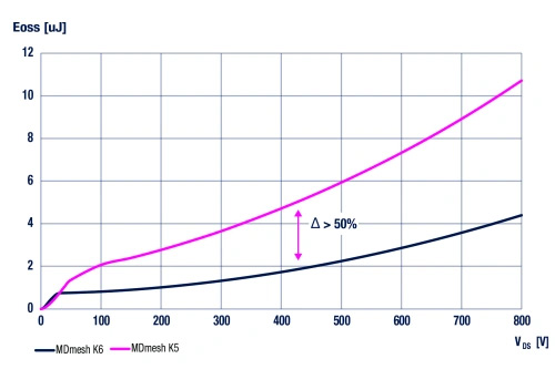
As already mentioned, one of the most important MOSFET device parameters – which plays a key role in the final performance benchmarking of the flyback converter – is the Eoss. Figure 5 gives an overview of the Eoss parameter, which is important mainly for switching losses. Compared to STs 800 V MDmesh K5, one can clearly see that the Eoss for MDmesh K6 is lowered by more than 50%.
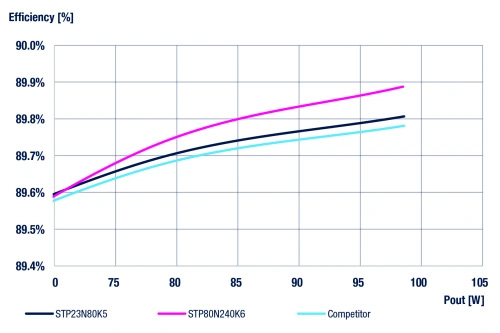
To give evidence of the good performance of the latest MDmesh K6 technology, Figure 6 shows the efficiency improvement in a 100 W QR flyback LED driver. This example compares the efficiency achieved using an MDmesh K6 MOSFET with that achieved using the previous MDmesh K5 technology and a competitor’s device. Simply by changing to a MDmesh K6 device, an efficiency improvement of 0.1% at full load can be achieved.
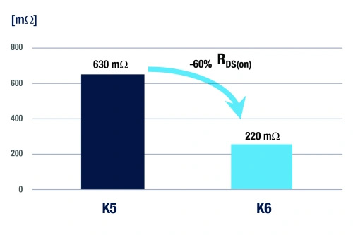
Nowadays, market trends are inclined towards the most compact and smallest power supplies. Hence there is demand for ever smaller and more powerful MOSFETs. MDmesh K6 addresses this needed, permitting more compact solutions that deliver increased system power density. In fact, MDmesh K6 enables MOSFETs to provide the same RDS(on) as the previous generation but in smaller package sizes. As indicated in Fig 7, MDmesh K6 has the best-in-class DPAK RDS(on) rating of 220 mΩ, which is ~60% lower than that of the previous ST technology, MDmesh K5. The DPAK packages help designers save space and hence increase power density when changing from through-hole devices to SMD packages.
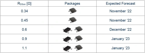
Following are some of the devices still to come in the MDmesh K6 family, which will provide extra flexibility for designers to achieve different power levels and hence fulfill a variety of application requirements.
Conclusion
The flyback converter is the most widely used topology for low-to-medium power applications. The choice of the switch and its parameters has a vital role in the final performance benchmarking. ST’s latest very-high-voltage super-junction power MOSFETs, in the MDmesh K6 family, offer a wide selection of RDS(on) with various package options that are optimal for applications such as LED drivers and device chargers that must combine high efficiency with compact dimensions and excellent reliability at a competitive price.