The WBG panel discussion focused on “the next wave of GaN and SiC,” taking its cue from the day’s topic presentations.
AspenCore’s PowerUP Expo 2021 devoted a full day to wide-bandgap (WBG) semiconductors, specifically gallium nitride (GaN) and silicon carbide (SiC). The WBG panel discussion focused on “the next wave of GaN and SiC,” taking its cue from the day’s topic presentations, including new product developments, technology challenges, and wafer manufacturing.
Thanks to their savings in size, weight, and cost, as well as higher efficiency, GaN and SiC power devices are making big pushes beyond fast chargers and renewable energy into data centers, motor drivers, electric vehicles (EVs), and other e-mobility applications.
The panel was comprised of six industry experts. Panelists in the GaN market included Alex Lidow, CEO and co-founder of EPC, who discussed GaN integration technology; Stephen Olivier, vice president of corporate marketing and investor relations at Navitas Semiconductor, who examined GaN’s role in electrification; and Caroline O’Brien, CEO of Kubos Semiconductor, who highlighted the company’s cubic-GaN technology for LEDs.
SiC panelists included Pete Losee, director of technology development at UnitedSiC (recently acquired by Qorvo), who discussed his company’s expanding portfolio with 750-V Gen 4 product series; Paul Kierstead, global director of power product marketing at Wolfspeed, who covered SiC’s role in renewable energy power conversion and storage; and Rob Rhoades, president and CTO of X-trinisic, who provided deep insight into SiC wafer manufacturing.
Common themes among the panelists included efficiency and integration, along with reducing the world’s reliance on fossil fuels with the help of WBG semiconductors. Panelists also agreed that the move to 200-mm wafers, coming soon, will be a further cost savings.
GaN: efficiency and carbon savings
Kubos’s O’Brien kicked off the panel with an introduction to the company’s new material technology, cubic GaN for LEDs. The next generation in lighting innovations is assumed to be the existing LED technology, but she counters that Kubos’s cubic-GaN LED technology could deliver a further 20% to 40% increase in efficiency. This translates into a carbon footprint and carbon savings of nearly 700 million tons of CO2 emissions over five years in lighting and displays, she said.
O’Brien said the new cubic-GaN can eliminate the inefficiencies in green and amber lights and offer opportunities in producing solutions that can be not only more efficient but also would improve color rendering and mimic daylight more effectively.
The “green gap,” or drop in efficiency in green and amber LEDs, is said to reduce the performance and increase the cost and size of RGBs. With cubic-GaN technology, the quantum confined stark effect and electric fields are eliminated, providing benefits in scale and longer wavelengths, and it delivers a reduced spectral drift, she said.
Similarly, GaN power device manufacturers like Navitas are focused on delivering technologies and devices that support electrification, which, in turn, reduce the world’s reliance on fossil fuels.
“Today, over 80% of the energy that becomes electricity is based on fossil fuels,” said Navitas’s Olivier. “One of the ways that we can improve that and shift from 20% renewables and electrical loads to 80% is by using GaN, which is a big push toward the electrification of our world.
“When we look at the small size of a GaN component and how we can integrate features and functions and reduce components from legacy systems, we can have up to a 10× smaller CO2 footprint than a silicon equivalent,” he said.
“Every time we ship a GaN power IC, we reduce 4 kg of CO2. That’s a huge net benefit by using new technology. We believe that we can accelerate the transition from internal-combustion-engine cars to EVs by three years worldwide and reduce road sector emissions by 20%, in all addressing a 2.6-gigaton-per-year reduction by 2050.”
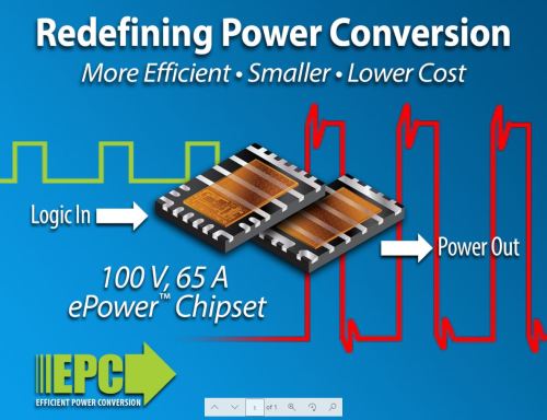
GaN power device manufacturers agree that the move from discrete GaN to higher integration will drive increased efficiency. Both Navitas and EPC discussed their integrated GaN products that deliver on improved efficiency, smaller size, and greater power output.
One example is Navitas’s GaNFast power IC with an integrated gate drive with GaNSense technology that integrates autonomous sensing and protection circuits.
The beauty of GaN is the integration of high-voltage, high-power, low-voltage, digital-logic, and other devices on the same chip, said Lidow. “The advantage of GaN is that it is extremely fast, and if you put a driver right on the same chip as the power device, you can get much higher speed than if they’re in two different chips. You also get advantages in terms of power efficiency.”
A few years ago, EPC introduced its fully monolithic power stage, which delivered much greater efficiency and greater power output. It also translated into a smaller size, fewer components, and less design time.
EPC expects to take the technology to a higher level of integration, and by the 2023/2024 timeframe, discrete power devices will start to fade out of EPC’s toolbox in favor of devices that have integrated functions on board, said Lidow. “For GaN, it’s about integration going forward.”
SiC: advances and savings
The benefits of SiC power devices are higher efficiency and higher switching frequencies. These features translate into smaller system devices, higher power density, and lower system cost. In addition, the higher switching frequencies are said to reduce the size of passive components.
Both Wolfspeed and UnitedSiC discussed the significant volume growth in the SiC market along with their latest product introductions.
A key part of Kierstead’s discussion centered on Wolfspeed’s SiC devices that are driving a change in renewable energy power conversion and storage.
A key advantage of Wolfspeed’s portfolio, as he sees it, is that the company covers applications from 6 kW to 22 kW on the charger side, which has been extended into the solar-based energy storage system (ESS) market.
“The benefits are certainly higher efficiency,” he said. “We can get higher switching frequencies. All of this drives smaller, lighter, system-level devices with better efficiencies, and along with the power density, it is allowing us to have lower system cost.
“We’re about 50% higher in power densities — so again, smaller, lighter, cooler — and we’re able to show about a net system cost benefit of 18%,” he added.
For UnitedSiC, a big part of its strategy is delivering low RDS(on). Losee devoted a portion of his discussion to its 750-V Gen 4 product series with 6-mΩ SiC FETs. Compared with a 650-V SiC MOSFET, the Gen 4 750-V FETs offer 3× lower on-resistance per unit area.
It’s about achieving the ultimate lowest RDS(on) per unit area by leveraging a normally “on,” very low-on-resistance SiC JFET with a low-voltage Si MOSFET, said Losee.
The company uses a slightly different approach to the SiC FET design, using cascode technology based on the SiC JFET. A key benefit cited compared with a standard SiC FET is the JFET’s superior transductance and good Idsat characteristics, which allow UnitedSiC to tune for short-circuit performance without large compromises in on-resistance under their nominal condition.
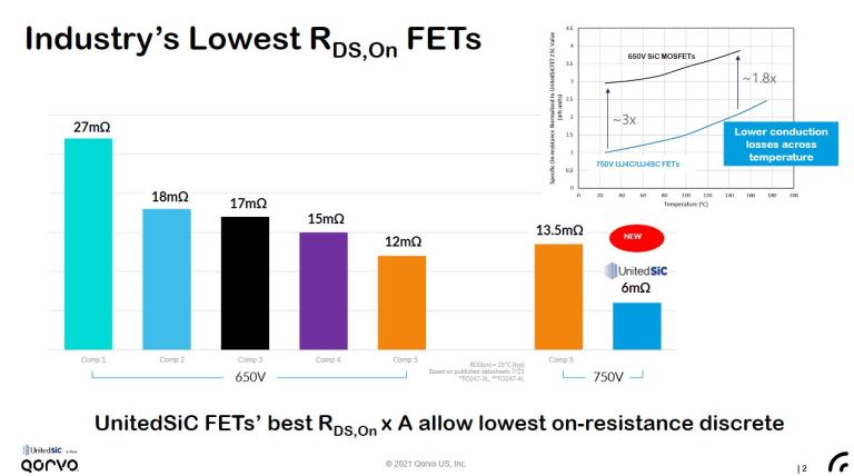
UnitedSiC also offers greater design flexibility with wider option ranges — in this case, an expansive portfolio from 6 mΩ to 60 mΩ with the 750-V FET.
With the full portfolio, designers don’t have to make large compromises in optimizing their system for efficiency, cost, or thermal management, Losee said.
X-trinsic’s Rhoades took a step upstream to discuss SiC wafering and the process sequence (and challenges) in the task of turning a single crystal puck of SiC into device-ready wafers.
SiC is unique in that it is an extremely hard crystal and it is also chemically inert, which makes it difficult to take through the sequence steps.
“You have to redevelop these processes with the properties of silicon carbide in mind, and each step will take longer and it will likely be more expensive,” said Rhoades.
As an example, “a lot of folks are now using slurries that are formulated around potassium and permanganate,” he said. “That is one of the innovations that has enabled SiC to now be available in reasonable quantities, and of course, everyone wants to reduce cost.”
Rhoades noted an inflection point occurring at 200 mm, with a transition to single-wafer processing. In the 100-mm to 150-mm wafer sizes, the traditional process sequence has involved batch polishing and batch lapping at the wafer-polishing and -shaping steps, and those are starting to show a geometric limitation when you get to the larger wafer sizes, which means you won’t be able to get as many wafers per batch, he said.
There is room for a lot of innovation in manufacturing methods to drive higher yield and lower cost that will benefit the overall industry, he added.