SiC and GaN technologies have grown tremendously over the years, demonstrating that they can hugely benefit power management
Silicon carbide and gallium nitride technologies have grown enormously over the past few years, proving to be commercially available energy-saving technologies. During the last “Wide Bandgap Devices and Applications Short Course,” a virtual event organized by PowerAmerica on Nov. 16–17, 2021, instructors coming from leading semiconductor companies, universities, and institutions have explained how wide-bandgap semiconductors enable clean energy manufacturing, high technology, job creation, and energy savings.
The first speaker, Peter Friedrichs, senior director of SiC at Infineon Technologies, has talked about SiC power device technology, focusing on aspects such as device design, reliability, and system benefits. According to Friedrichs, SiC has still a substantially higher price than silicon, mainly due to the substrate (wafer) manufacturing process and to its higher defect density. However, by using multiple substrates and dropping down the defect density, Infineon has been able to reduce the overall production costs.
“The more cells, or the more channel widths, you can place into a given area, the more efficient your device becomes; it means also the concept that the best volume utilization is favored,” said Friedrichs.
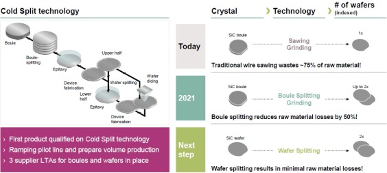
The first step, which is already productive now on Infineon sites, has been achieved through the innovative Cold Split technology, which can process crystal material efficiently and with minimal waste of resources. Today, traditional wire sawing wastes up to 75% of raw material, while the already-deployed SiC boule splitting is able to reduce raw material losses by 50%. In the near future, Infineon will use this technology to split entire SiC wafers, thus doubling the number of chips out of one wafer, as shown in Figure 1.
In SiC planar MOSFETs, the channel resistance is normally pretty high. That means we can achieve a low on-resistance as a final device only if we apply a significantly higher electric field across a gate oxide. Today, nearly all common MOSFETs have more than a 3-MW/cm electric field applied to the gate oxide. Planar is relatively easy and cheap processing that allows you to achieve a very good shielding of the gate oxide in blocking mode. However, it has lower channel mobility and limited device area shrink options. On the other side is the trench design, which brings benefits such as lower on-resistance, smaller parasitic capacitance, and improved switching performance. The drawback, however, is a reduced short-circuit tolerance due to the lower on-resistance.
“SiC system benefits and value propositions, which we believe are striking and unique, include the solar inverter — with a significant increase in power-handling capability while keeping volume and rate nearly constant — motor drives, and EV charging, especially with the ultra-high–power charging up to 350 kW, very high voltages, very high currents, and fast switching,” said Friedrichs.
The next speaker was Victor Veliadis, executive director and CTO of PowerAmerica, who talked about the SiC market outlook and some of the key applications. Power devices are large discrete transistors capable of switching high currents and blocking high voltages. The critical electric fields and energy gaps for SiC and GaN are much higher than those of silicon. Because breakdown voltage is inversely proportional to the critical electric field, if we increase the critical electric field tenfold, the thickness of this drift layer becomes 10× smaller, reducing the resistance of the device we are fabricating. For a specific breakdown voltage, the resistance will be proportional to the inverse third power of the critical electric field. So if we have a critical electric field that is 10× bigger, the resistance contribution of this layer will be 1,000× smaller.
“Large critical electric fields allow you to make high-voltage devices with much thinner layers than what you would have in silicon,” said Veliadis. “That reduces the resistance, the associated conduction losses, and the overall capacitance. That allows you to operate at higher frequencies and temperatures, with higher efficiency, and it simplifies a lot of the magnetic circuits, the volume, the weight.”
While silicon is still competitive at lower voltages up to 650 V, SiC and GaN offer efficient high-frequency and high-current operation at higher voltages. The big battleground among Si, SiC, and GaN plays around 650 V, where all the devices are suitable for the 400-V EV bus voltage.
“Looking at some of the opportunities, the first one is automotive with the electric vehicles,” said Veliadis. “UPS for data centers is another big area where silicon carbide can play a significant role. Other applications include green infrastructure — basically, photovoltaic and wind energy — electric motor drives, micro grid, and fast-charging stations. This is where 6.5-kV and 10-kV MOSFETs are going to be needed.”
The SiC device market is projected to be a $3.2 billion market by 2025, with a phenomenal CAGR growth over the years, up to 50%.
Wide-bandgap devices can be of a lateral or vertical configuration (see Figure 2). The larger the separation between drain and gate, the higher the breakdown voltage the device can tolerate. However, if we increase this distance so much, the device will take up too much space on the wafer, increasing the overall cost. The solution is to go vertical. Instead of having a large gate to drain separation in the horizontal direction and take up space on the wafer, we do that in the vertical direction. That’s the reason why the vast majority of SiC devices have a vertical configuration.

Burak Ozpineci, section head for vehicle and mobility systems research at the Oak Ridge National Lab (ORNL) in Knoxville, Tennessee, gave a presentation on power electronics for EVs. “We are still focused on pure EVs and looking at electric vehicles going beyond the 200-mile range, with 60-kWh or higher energy storage,” he said. “We are currently looking at ways of integrating the motors and power electronics inside the chassis.”
ORNL’s roadmap defines the pathway to achieving 2025 targets, which consist of an increase of the power density, power level, and vehicle reliability/lifetime, halving the total cost per kilowatt. Ozpineci has presented five major keystone projects developed at ORNL in this area:
- Look for technologies that help us achieve higher power densities. These technologies include new materials and substrates (such as insulated metal substrate with insertion of thermal pyrolytic graphite or direct bonded copper), a genetic algorithm for heatsink optimization, and reduction of volume for DC-link capacitors.
- New topologies for electric motors. Because ORNL is provided with a supercomputer facility, it can be used to generate a high-fidelity model of the motor, such as the outer rotor motor, which has the stator inside and the rotor outside.
- The outer rotor motor integrates the inverter right into the motor, eliminating the connectors and long cables and reducing the size of the motor by up to 30%. This is the third keystone project; that is, the integrated electric drive.
- Medium-duty and heavy-duty electric drives. This project aims to extend the research area from passenger vehicle electric drives and component technologies to medium-duty and heavy-duty electric drives. That means higher-voltage batteries (1,000–1,500 V), higher current levels, and higher power requirements for charging (greater than 1 MW).
- Wireless charging. Right now, the research is focused on 200-kW–plus stationary or static wireless charging. The goal is to go to 270 kW, a power level that can be achieved only with SiC devices, looking also at dynamic wireless charging.
Iqbal Husain of North Carolina State University has talked about wide-bandgap power electronics driving high-speed electric machines for EVs. The four major areas of power conversion that are used in the electric powertrain are the inverter, the DC/DC converter, the converter that supplies the low-voltage electronics, and an on-board charger. So SiC devices offer this opportunity for enabling either smaller batteries or longer driving range with smaller, cooler, and lighter systems in the various converters.
“In all of these areas, there is the opportunity for using silicon carbide devices because of the advancements and the stage they are in, in terms of their availability and commercial production,” said Husain. “Our ultimate goal is to improve both the efficiency and the power density.”