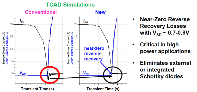
This new silicon power mosfet offers near-zero reverse-recovery losses, bringing an advantage to silicon that is usually seen only in gallium nitride technologies while maintaining the cost and compatibility advantages of silicon.
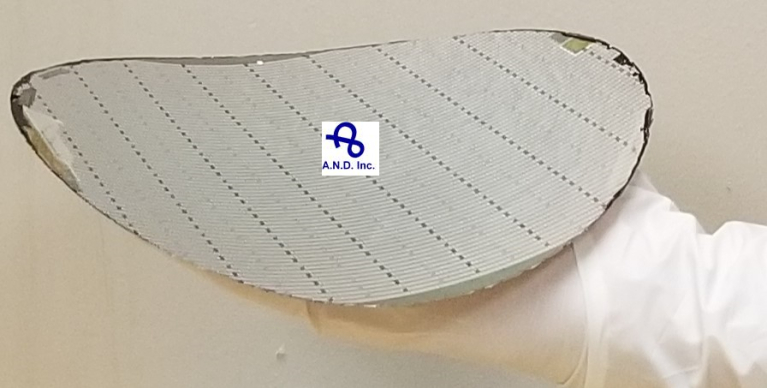
Applied Novel Devices (AND), a provider of new semiconductor device architectures applicable to discrete and integrated power devices, has introduced a major industry breakthrough with its new class of silicon power MOSFET (ANDFET) technology, which features a sub-30-µm substrate that offers significant benefits for fast-switching and power-conversion applications. These parts are manufactured at SkyWater Technology, a U.S.-owned semiconductor manufacturer and a DOD-accredited Trusted supplier. This new technology offers near-zero reverse-recovery losses, bringing an advantage to silicon that is usually seen only in gallium nitride technologies while maintaining the cost and compatibility advantages of silicon. ANDFET reduces form factor for both standard products and multichip modules with a novel wafer-scale packaging and enables higher-frequency power-conversion applications that can also shrink module form factors.
Power transistors
Standard silicon power transistors have features that are lithographically defined, vertical thickness that is limited by handling and process complexities, and parasitic diodes that contribute to reverse-recovery losses. The ANDFET addresses all these limitations using self-aligned vertical MOSFET architectures to push lithographic limits and increase power density, novel thin crystalline processing that yields mechanically rugged sub-30-µm silicon in production-ready 8-inch wafers, and elimination of parasitic diodes to near-ideal reverse-recovery characteristics.
Remarkable innovations have been implemented by the team at Austin, Texas-based AND, established in 2008 to enable the continuation of silicon power MOSFETs in mainstream applications. The team includes Leo Mathew, CEO and co-founder, who was the EE Times Innovator of the Year in 2006 while at Freescale Semiconductors for his innovation of the ITFET, which demonstrated both vertical and horizontal channel regions for CMOS devices.
At this year’s APEC, AND showcased its new class of Si power MOSFET that provides high-efficiency power conversion. Mathew and select members of AND attended APEC, including Rajesh Rao, CTO; Kevin Lally, a semiconductor industry veteran, board director, and early investor/advisor; and Vishal Trivedi, director of technology and co-author of the book “Fundamentals of Ultra-Thin-Body MOSFETs and FINFETs.” Trivedi presented the work on ANDFET technology at APEC and introduced a new 20-µm–thick silicon with GaN-like performance in volume manufacturing at an 8-inch wafer foundry. This technology is initially targeted at battery protection, load switches, and for the DC/DC converter market in the 15-V to 100-V range.

“If you look at a GaN device, the biggest advantage in addition to on-resistance [RDS(on)] is the switching performance, especially the [near-zero] reverse recovery, but we have demonstrated that we can do this in silicon,” said Mathew. “Because it is only 20 µm thick, you also make the on-resistance component of it very low.”
In the industry, designers consider adding a Schottky. “If you add a Schottky, it becomes much leakier, and of course, sub-threshold slope is bad,” said Trivedi. “We don’t need a Schottky to eliminate reverse recovery, and it has very low leakage, with a very good sub-threshold of 60 mV.”
AND power MOSFETs
Power MOSFETs are discrete transistor devices specifically designed for switching high-voltage and high-current signals and widely used in power applications in industrial, automotive, and consumer applications. The demand for high-efficiency power solutions is increasing in these areas, which poses further challenging requirements such as high switching frequency, reduced footprint and weight, and better thermal management.
According to AND, the new class of Si power MOSFET developed has the following advantages:
- Near-zero reverse-recovery losses, a great achievement for a Si-based device (usually seen only in wide-bandgap technologies, such as GaN)
- Reduced form factor, for both standard devices and multichip modules, obtained through a novel wafer-scale packaging
- Higher operating frequency in power-conversion applications
- 2× lower output charge
- Ultra-low QOSS
- Low leakage current
- Near-ideal sub-threshold slope
- Low specific on-resistance (as low as 5 mΩ/mm2 at 30-V BVDSS)
- Low gate drive, as low as 2.5 V (logic-level drive)
- Sub-30-µm substrate, built with thin crystalline technology
A low RDS(on) and near-zero reverse recovery enable higher efficiency and contribute to reduce both the number of components and the overall cost of the solution in applications such as power supplies and motor control. Performance of soft and resonant switching applications can also be improved thanks to a combination of low RDS(on), low gate drive, and low output charge. Moreover, the thin body design provides an excellent thermal management and better immunity to temperature variations and might help to achieve inherent radiation-hardened characteristics.
According to Mathew, AND has developed a unique technology that brings the benefits of GaN-like performance to mainstream Si MOSFETs.
The transfer characteristic curves, referred to a device based on AND’s novel technology, an industry device, and an industry device with a Schottky body diode, are shown in Figure 3. According to Mathew, ANDFET features an industry-record, near-ideal sub-threshold slope, a low gate-drive voltage, and low leakage current.
GX0WTL6FZH.png)
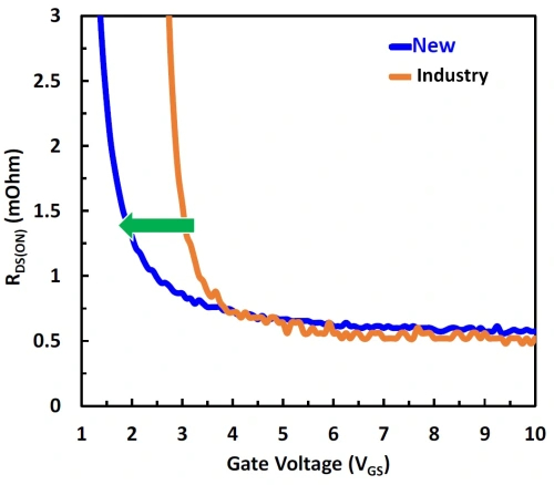
A comparison between the on-resistance characteristics of the ANDFET and an industry power device is shown in Figure 4. Here, we can see how the ANDFET, compared with a traditional one, exhibits lower RDS(on) and very low gate drive (approximately 2.5 V, corresponding with a logic-level voltage).
AND’s proprietary channel engineering technology provides outstanding qualities that can help power management systems cut parasitic losses significantly. This will increase power management and conversion efficiency in a variety of applications in the industrial and consumer markets, including data centers, automobiles, electric motor drives, microinverters for renewable energy systems, and many more (Figure 5).

According to AND, its technology offers distinct advantages in applications like DC/DC power converters. Moreover, integrated, or independent, Schottky clamp diodes are not required due to the near-zero reverse recovery and low output capacitances. These efficiency-boosting features make the technology appealing for higher-frequency voltage-conversion applications that aren’t normally handled by traditional Si-based MOSFETs. As a result of the high frequencies enabled by these power MOSFETs, passive component sizes are reduced, resulting in tiny-form–factor power modules that facilitate further system-level efficiency advances (Figure 6).
Earlier this year, AND and SkyWater announced that the companies have entered into a licensing and manufacturing agreement to deliver the new transistor technology that offers significant benefits for fast-switching power-conversion applications.
Headquartered in Bloomington, Minnesota, SkyWater will produce Si power devices based on the novel technology, allowing AND to offer wafer-scale and standard package products ranging from 15 to 80 V for industrial and consumer applications. AND intends to expand its product line to include a family of products for electric vehicles, renewable energy, and different industrial applications, spanning the voltage range of 200 to 1,000 V. AND is also working on implementing its proprietary device architecture in SiC and GaN to address some of the challenges and further improve its performance.
In terms of product availability, AND is sampling the new ANDFET and is about to begin high-volume manufacturing at the SkyWater 8-inch fab. Wafer-scale devices will be customized to precise form factors for current boards and systems. The products are available from AND, and the technology is currently a foundry offering from SkyWater.