GaN offers lower conduction and switching losses that enable higher switching-frequency operation at high efficiency adapters.
The landscape for power adapters used to power everyday electronic devices ranging from phones to laptops has changed considerably since the introduction of USB-PD specifications and through its evolution. While USB-PD ensures wide-ranging compatibility, the power adapter design becomes somewhat more challenging: now, the power adapter has to support a wide range of output voltages (as opposed to a single output voltage for captive use adapters). Meanwhile, the end user’s desire for lighter, smaller adapters continues. Gallium nitride power switches have been introduced in recent years to address these dual requirements.
GaN devices offer lower conduction and switching losses compared with silicon devices that enable higher switching-frequency operation at high efficiency, hence lighter and smaller adapters. GaN-device–based designs require special attention because the gate voltage range is limited and the gate is susceptible to spurious turn-on and turn-off. However, GaN FETs with monolithically integrated drivers such as the TP44x00NM series from Tagore Technology make the implementation robust and easy in addition to offering space savings.
While GaN devices enable higher power densities, there are still some system-level issues to resolve to achieve a highly reliable and marketable adapter design. As every power electronics engineer knows, these center around thermal design and EMI compliance. As human beings, we work hard to stay cool and calm when we are in tight situations. The story is no different for the circuits we design: The electronics within the adapters have to stay cool (exhibit low temperature rise) and calm (low emitted noise) in the tighter spaces we are placing them. We look at the techniques to achieve these goals in this article.
Thermal and EMI challenges
Thermal and EMI design challenges are not new to power supply designers. However, with the tighter spaces enabled by GaN technology, these challenges become exacerbated.
Focusing specifically on the GaN device, the die size of a GaN device is much smaller than that of an equivalent power-loss–performance silicon device. Also, GaN-device packaging is smaller, requiring special measures to limit the die temperature. Even when the GaN device has lower losses, the enhanced thermal-management challenge remains. From an EMI point of view, GaN devices have lower parasitic capacitances, so they tend to switch with faster rising and falling edges, which can lead to the generation of harmonics and EMI.
Additionally, the tighter arrangement of components in a denser adapter is antithetical to achieving low temperature rise and EMI. The proximal heating between more dissipative components and others can lead to higher temperature-rating requirements on the other components. Also, the fully enclosed packaging of adapters offers limited options for heat dissipation. From an EMI point of view, the proximity of switching devices and smaller primary-secondary spacing can lead to cross-coupling and other problems.
Despite the above-mentioned challenges, there are techniques available to designers that can lead to improved thermal and EMI performance.
Thermal solutions
The basic principle behind effective thermal management is to distribute heat in the most efficient manner. This can be achieved in multiple ways, including strategic layout placement of components; increasing heat spread through the PCB by adding copper planes to connect to heat-dissipating components; adding copper plating to the inside surface of the enclosure; and using thermal-gap filler material to bridge the PCB top and bottom.
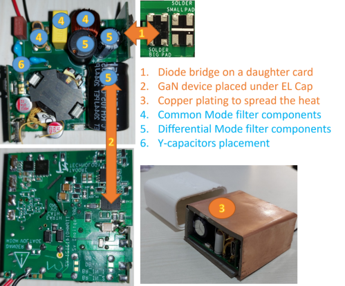
We will take the example of a 65-W adapter design using quasi-resonant flyback (QRF) topology to illustrate the ways to implement some of these concepts. First, it should be recognized that the input electrolytic filter capacitor (EL cap), which is large in volume (about 15% of the adapter volume) dissipates very little heat. So it helps to place the GaN device directly underneath the EL cap on the opposite side of the board. Using vias and thermal glue to transfer the heat to the EL cap side of the board helps significantly. A similar strategy can be applied with EMI filter inductors and other dissipative components.
Another helpful step is to move the input bridge rectifier (that dissipates 4.5% of the output power) to a daughterboard. Self-heating of the rectifier components is not detrimental to the adapter performance. However, the heat spread from the rectifier to the GaN device can impact the power-handling capability. Finally, before assembly, copper plates can be strategically used to connect areas with high dissipation to areas with low dissipation and try to equalize the temperatures within the adapter. Figure 1 illustrates some of these concepts.
EMI solutions
EMI solutions include traditional approaches, such as choosing the right frequency, proper layout, selection of appropriate EMI filter, and controlling switching transitions. The QRF topology allows for softer turn-on switching transition, and that helps reduce EMI. The TP44x00NM series also allows control of the gate turn-on speed that provides an additional lever to limit EMI.
The primary-secondary capacitance in these tiny adapters is much higher, as the spacing between primary and secondary sides is reduced from the customary 8 mm to a lower level. This reduces the common-mode impedance and leads to higher levels of coupling between the primary and secondary — the copper foils for spreading the heat make this phenomenon worse. The eventual conducted EMI compliance requires several special measures (some highlighted in Figure 1). First, the common-mode (CM) choke needs to be split into two inductors (one for frequencies to 1 MHz, the other for 1–30 MHz) on either side of the X capacitor and placed on the AC side. The differential-mode (DM) filter is a pi filter formed by splitting the DC-side filter cap into two and putting a DM choke in the middle. Finally, and most critically, the Y capacitor, which is constrained by safety requirements, is placed in two locations. One (680 pF) is placed between the X capacitor and secondary ground, and the other (also 680 pF) is placed between the secondary switched node and primary ground. The total value of 1.36 nF is much lower than the 2.2-nF Y-capacitor limit — offering some design margin.
End results: thermal and EMI improvements
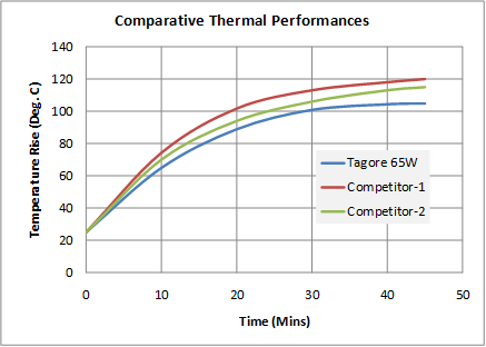
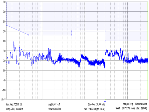
The thermal and EMI improvement measures described above were implemented in an adapter that was then compared with similar commercially available adapters that also use GaN technology. The thermal and EMI results are shown in Figure 2 and Figure 3, respectively. The thermal performance of the adapter using the TP44200NM stabilized earlier with the implemented improvements, and the end temperature was at least 10˚C lower than the other adapters. The EMI performance was also superior to the market-sourced adapters (plots not shown) and provided >10-dB margin to the limits throughout the frequency spectrum.
Conclusion
The implementation of GaN-based adapters can be made more robust with the techniques covered in this article. The underlying performance benefits of GaN and GaN ICs are further enhanced by closer attention to component selection, board layout, and packaging techniques. When the electrical, thermal, and EMI performances are harmonized, the result is likely to be not only a cooler (low temperature rise) and calmer (low EMI) adapter but also a cooler and calmer professional experience for the design team.