We report some studies of the different switching- and voltage-loss configurations in a cryogenic environment for GaN devices.
Gallium nitride power devices are used in an increasing number of applications due to their excellent performance. This article explains the main characteristics to consider. A possible study is GaN for cryogenic applications, such as aviation, space, and superconducting systems, particularly the working conditions below the temperature of liquid nitrogen (77 K) in different circuit configurations. In this paper, some studies of the different switching- and voltage-loss configurations in a cryogenic environment are reported. The authors investigated the performance of four commercial GaN devices over a wide temperature range between 400 K and 4.2 K. According to the authors, as reported in the original article, all tested devices can successfully operate at cryogenic temperatures with an overall improvement in performance. However, different GaN HEMT technologies imply significant variations in device gate control.
GaN HEMTs
In this blog, we discussed GaN’s improved performance compared with silicon in a variety of applications in which the temperature can approach 150˚C. Many applications, however, need devices that can operate at temperatures as low as a few Kelvin — consider new energy uses, energy storage, superconductors, and aviation and space applications.
With a major increase in cost and structural complexity, power systems are often insulated and kept at ambient temperatures. As a result, operating the system directly at the temperatures involved would be quite favorable.
When the temperature drops in silicon and wide-bandgap devices like silicon carbide and vertical GaN, two significant phenomena emerge, as mentioned in the article: Carrier mobility rises as the electron-phonon interaction, a high-performance parameter, diminishes. Furthermore, this drop is mirrored in a fall in carrier density, which leads to an increase in channel resistance and a shift toward positive threshold voltage (Vth) levels.
Because the carriers are created by the polarization mismatch between the AlGaN barrier and the GaN layer, GaN HEMTs do not require any doping to attain a high concentration of electrons in the channel. The temperature has no bearing on this occurrence.
Characterization evaluations of commercial devices (EPC and GaN Systems) have been published in several research papers, demonstrating the rise in performance up to temperatures of 77 K. The authors of this work look at the performance of standard GaN topologies, including the gate injection transistor (GIT) and cascode, as well as features like device conduction and soft- and hard-switching losses, from 400 K to 4.2 K. The devices considered in the original IEEE article are shown in Figure 1.
Figure 2 shows the scheme used by the authors to carry out the measurements. The temperature varied between 400 K and 4.2 K with a tolerance of 0.1 K using a PID controller, and the measurements were carried out under vacuum conditions (10E-4 mbar at 300 K).


Basically, four commercial devices were described and compared, each with identical currents and voltages but distinct device technology. To offer DC device and switching characterization at the same time, two transistors were employed. A 10-nF (multilayer ceramic) Cref capacitor was attached to the gate and source terminals of one device to perform Sawyer–Tower (ST) tests to evaluate device switching losses (Figure 2). For more details about the ST method, read this article.
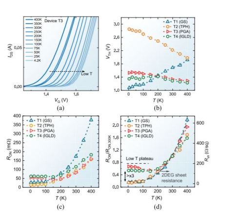
The transfer function, and hence the positive shift in the characteristic, may be observed in Figure 3 from the authors’ study. On the other hand, the threshold voltage, based on 1-mA Ids, indicates a significant difference between the solutions. As the temperature drops, the Vth of the GIT devices (T3 and T4) remains relatively constant but slowly rises. The Cascode exhibits a significant rise, but the circuit’s resilience allows it to be driven with high gate voltages (Vg), compensating for the Vth drift. Vth drops from 1.6 V at ambient temperature to 1 V at 4.2 K for T1. This impact may result in a smaller “off” state margin and, as a result, fewer false positives. This effect could ensure a reduced “off” state margin and thus false positives under those conditions.
The drop in temperature seen in Figure 3c indicates a reduction in the device’s on-resistance. This is due to a reduction in resistance caused by increased electron mobility. However, this behavior differs among the four devices, indicating that they are all tied to HEMT technology, as seen by the graph of the normalized value (d in Figure 3) realized by the authors. Such disparities in behavior between technologies have a direct influence on device conduction, losses, and the drive circuit.
Depending on the operating conditions of the circuit, the devices are subject to soft- or hard-switching losses. Soft is typically characterized by an ST measurement and related to the non-ideal charge and discharge of the device’s output capacitance (Coss) and becomes important at high frequency. The measurement of the voltage across the reference capacitor (Vref) allowed Qoss to be obtained and thus the energy dissipated at each switching cycle (Ediss) considering the hysteresis cycle between the charge and discharge paths.
They all react differently, as indicated in the article, implying that this variance is tightly tied to the specific energy level of the trapping sites. Because each manufacturer often uses its own structure, the switching-loss values and temperature behavior should differ greatly depending on the GaN buffer mix and Si substrate used. In comparison with conduction losses, soft-switching losses have a moderate temperature dependency, according to the authors.
Hard-switching losses are very difficult to measure in this context. The main contribution is represented by f × Eoss (where f is the switching frequency and Eoss is the energy stored in the output capacitance of the transistor at a certain value Vds in the “off” state) and another bound term associated with the external load current flowing from the circuit through the device channel during Coss discharge. As shown in the graphs in the original article, the contribution of Eoss to the hard-switching losses is fairly constant over a wide temperature range (a larger variation for T4).
From the analysis, it can be seen that all tested devices can operate at cryogenic temperatures. Different GaN HEMT technologies undergo variations that need to be considered during design.