Hexagem is developing a GaN solution at the Swedish research institute RISE testbed ProNano.
The GaN semiconductor is a key component of future energy-efficient electric vehicles and 5G networks. Hexagem, a Lund, Sweden-based startup, is developing a solution at the Swedish research institute RISE testbed ProNano that aims to contribute to greater electrification and a sustainable future.
In an interview with EE Times Europe/Power Electronics News, Mikael Björk, CEO at Hexagem, and Michael Salter, senior project manager at RISE, pointed out the importance of this collaboration, which will lead to Hexagem’s technology being implemented in future energy applications.

“They’ve demonstrated their technology on a small scale in the research labs, but now they’re transferring the process to larger wafer sizes in larger volumes in our laboratory to try to scale up the technology,” said Salter.
“The advantage that ProNano gives us is that Hexagem gets access to a state-of-the-art facility and tools, in particular an MOCVD1 capable of 6” wafers,” said Björk. “Typically, this type of tools is difficult for startups to finance on their own. In addition, RISE personnel has deep experience with GaN materials, processing, and characterization.”
Industry
Industry sectors ranging from automotive to telecommunications are being pushed to invest in more efficient power conversion and more electrification as societal pressure and regulation for lower CO2 emissions grows. Traditional Si-based power semiconductor technologies, such as insulated-gate bipolar transistors (IGBTs), have basic limitations in terms of operating frequency and speed, as well as poor high-temperature and low-current performance. The frequency and high-temperature performance of high-voltage Si FETs are similarly restricted. As a result, WBG semiconductors are becoming more popular in many applications.

GaN power semiconductors are gaining traction as a key component in the next generation of high-performance EVs, helping to reduce size and weight while increasing efficiency. These considerations address concerns with range. Engineers may use GaN to create power electronics systems that are 4× smaller and lighter and have 4× less energy loss than Si-based systems. Zero reverse recovery, which reduces switching loss in battery chargers and traction inverters, as well as higher frequency and quicker switching rates are among the benefits. Furthermore, decreased switching turn-on and turn-off losses can aid in the weight and volume reduction of capacitors, inductors, and transformers for applications such as EV chargers and inverters.
GaN wafer
Next-generation energy-efficient semiconductors will help create new solutions for a sustainable future. This means less carbon dioxide emissions and thus improvements in global warming in the long run. Predictions from many agencies indicate that electricity use will increase to more than 200 TWh by 2050, a high number that requires attention at the design level.
Semiconductor substrates, or rather wafers, have the goal of controlling the electrical current and the performance of the entire end device. Round wafers are cut into postage-stamp-sized pieces encapsulated in microchips containing millions of transistors.
Most semiconductors are made of silicon, but different variants are being developed to meet the need for greater efficiency in energy applications. For example, in a car, more than 1000 chips are required, and the number is likely to grow. Future developments in semiconductors will allow more transistors to be contained by facilitating integration.
Hexagem develops semiconductors with gallium nitride on silicon wafers. Hexagem’s development activities for high-quality GaN-on-silicon are aimed at reducing the cost and scale advantages of future applications. They are looking at higher requirements in terms of voltage rating. According to Hexagem, the offered technique would keep costs low by leveraging the existing infrastructure.
GaN-on-Si technology does not have a good reputation in terms of development. It has its challenges, and growing GaN-on-Si is not easy due to the mismatch of material properties at the interface on the atomic scale between GaN and Si.
“The key advantage and challenges for the technology will be to provide lower defect densities and increased GaN thickness to enable 900-1200V power devices,” said Björk.
Manufacturing organizations are increasingly relying on their capacity to design both the product and the supply chain at the same time. One of the primary advantages of GaN-on-Si is that it is manufactured on silicon substrates, so it is now 150 mm wide, with plans to expand to 200 mm, and most reactors can accommodate both.
Defects
During semiconductor epitaxial material manufacturing, dislocations, i.e., defects in the material, are created. The more defects in a semiconductor the fewer useable devices on a wafer can be produced, which increases the cost. In addition, poor material interfaces cause higher device channel resistance which causes more energy to be wasted during operation, making the chip less energy efficient.
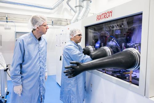
“We have installed and operate a MOCVD reactor for growing the GaN material on the silicon wafer,” said Salter. “We’re investing in this equipment and infrastructure which requires additional equipment and specialized process utilities, like gases and cooling water. Growing the GaN material with low defect density is one of the biggest challenges for gallium nitride applications, as well as controlling material quality during the deposition process. Controlling the base material and dopant concentrations during the deposition process allows for low resistance device contacts to be achieved at the device level. This also affects the types of breakdown voltages and current levels that devices can withstand. In addition, having a good interface between the semiconductor material and device contacts helps optimize electrical performance of the manufactured device.”
RISE Test and Demonstration Facility ProNano offers a variety of infrastructure to help speed up startup testing without having to spend a lot of money on expensive equipment. Nanowires are manufactured using ProNano’s metal-organic chemical vapor deposition (MOCVD) technology to produce thin gallium nitride layers on the silicon wafer. The wafers are treated and confirmed at every level to produce patterns in which the gallium nitride nanowires may “grow” and then coalesce together to produce high-quality thin epitaxial layers. The wafer is then examined under an electron microscope to check its quality.
According to Hexagem, at present GaN-on-silicon semiconductors have 100 million defects per square centimeter. “This would be a dislocation density of the order of 108 cm-2. State-of-the-art GaN-on-Si wafers today is mid-to-high 108 cm-2,” said Björk. Hexagem believes that we can significantly improve the material quality, soon approach 10 million defects per square centimeter and thus surpass the competition.
“Defects are generally dislocations that cause off-state leakage,” added Björk. “With Hexagem technology, we are able to reduce dislocations in two steps; firstly, by filtering GaN buffer dislocations by growing GaN nanowires, and secondly, by careful coalescence of the wires into planar GaN layer controlling formation of new dislocations.”
Vertical wafer
The goal is to have larger wafers or to produce thicker vertical gallium nitride semiconductors. According to Hexagem, two to four micrometer-thick layers are common today. Their goal is to produce ten-micrometer-thick solutions in 2022.
“Larger wafers mean improved economy of scale by increasing the number of devices per wafer,” said Björk. “The disadvantage is that it is typically more difficult to control wafer bow on larger wafers. Thicker GaN layers will enable devices with higher voltage ratings, which will be important for addressing 900-1200V device markets. It would also enable vertical device design, which would bring benefits such as decoupling voltage scaling from device footprint. Hexagem aims at developing high-quality GaN-on-silicon for 1200V device designs and licensing the technology to industrial partners.”
Hexagem said its technology allows the current to flow vertically instead of horizontally on the wafer plane. This reduces the size of the components, but more importantly, it can handle even higher currents and voltages.
Semiconductor processing
As indicated above, MOCVD (Metal-organic Chemical Vapor Deposition) is the primary procedure for making transistors from semiconductor materials with a large bandgap. Specific gases (or vapors) flow at specified temperatures and pressures across the surface of the substrate in an MOCVD system. The top layers are “developed” into a crystalline structure in this way, one atomic layer at a time, across multiple layers. The technique is known as epitaxy or crystalline growth. To create 3D nanostructures such as nanowires, layers can be grown over the full surface of the substrate or over selected sections of the substrate.
Epitaxial layers can be grown using the MOCVD process on substrates of different materials such as silicon, silicon carbide, gallium nitride, diamond, or sapphire. The materials have different degrees of difficulty to obtain few crystalline defects.
Next, the wafer transistors and other electronic components are created by additional processing steps common to semiconductor fabrication, such as lithography, etching, or metal or insulator deposition. Finally, the finished wafer is cut into postage-stamp-sized pieces that are encapsulated in an electronics package, tested, and sent along supply chains, for example to Samsung, Volvo, Apple, and Ericsson, and finally, end up in a microprocessor in a cell phone or a car.
The major phases in creating GaN wafers on silicon are substrate washing, followed by pattern growth in a clean environment, and further substrate cleaning during pattern growth. The next step is the creation of GaN semiconductors via MOCVD epitaxy. Based on a specific technological need, the substrate is put in the MOCVD chamber to produce crystal layers in different combinations of GaN, AlGaN, or InGaN. After that, an electron microscope is used to examine the material, and tests are carried out to validate the material’s electrical conductivity and other properties.