Applications with high-current requirements such as battery isolation and motor drive require careful consideration of design requirements.
Applications with high-current requirements such as battery isolation and motor drive require careful consideration of design requirements. It’s important to understand maximum ratings in circuit design to get the best performance from power MOSFETs and maintain device reliability during the required operating life. Maximum ratings must not be exceeded in order to guarantee device longevity and dependability.
Modern electronics using low-voltage (<100-V) MOSFETs have seen an increase in demand for high power in both automotive and industrial applications. Power output in terms of kilowatts for applications such as motor drive is now a very common requirement. Combined with today’s module space constraints, this means that the need to handle more power is being passed on to components, particularly MOSFETs.
During Nexperia’s Power Live Event, Stein Hans Nesbakk, application engineer, and Steven Waterhouse, international product marketing manager, both at Nexperia, highlighted the need for the correct evaluation of the drain current and the possible use of protection circuits to compensate for high-current events and thus offer a highly reliable product. The drain current (ID) limit indicated in the datasheets of power MOSFETs is one of the most important parameters in such high-power applications in which the management of very high currents is required.
ID rating
The MOSFET has three terminals: gate, source, and drain. Current can flow via any of these terminals, which are labeled IG, IS, and ID. Engineers and electrical designers must thoroughly comprehend the essential capabilities, constraints, and environmental circumstances to pick the appropriate MOSFET for the application.
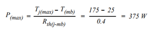
ID is the maximum continuous drain-source current that the MOSFET can sustain while fully enhanced at Tmb = 25°C and die at max junction temperature. As the speakers noted, it is a single parameter but captures thermal performance, temperature rating, RDS(on), silicon die resistance and package resistance. The maximum current that a MOSFET can achieve is primarily derived from the maximum power allowance in the MOSFET. When calculating maximum continuous current, the maximum steady-state power must be used. If we define Tmb = 25°C, Tj(max) = 175°C, and Rth(j-mb) = (0.4 K/W max), we can calculate the maximum power as follows:
The key parameters needed to calculate this maximum power allowance are the thermal impedance between the die and the mounting base Zth(j-mb) (Figure 1) and thermal resistance between the die and the mounting base Rth(j-mb). Rth(j-mb) is the thermal resistance that refers to the thermal response that has reached steady-state conditions (also referred to as DC conditions).
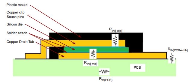
Rth(j-mb) is the thermal resistance from junction to mounting base. The transient thermal resistance from junction to mounting base is as a function of pulse duration as shown in Figure 2. As can be seen, the MOSFET thermal response is similar to an RC network electrical response. Its thermal resistance varies depending on the kind of pulse delivered (single-shot or repeated PWM pulses with varying duty cycles), and for pulses longer than 10 ms, the curves begin to plateau and flatten after 100 ms, as seen in the graph. The MOSFET is said to have reached thermal stability at this point. So from the MOSFET’s perspective, it’s in a thermal DC. Although the thermal resistance stabilizes after 0.1 seconds, Nexperia test all MOSFETs in a lab for 30 seconds or more. The 175°C temperature refers to the junction temperature of the MOSFET, and the parameter for this is given as Tj. All MOSFETs must operate below this temperature. P(max) can be found in the datasheet limiting values table. Using the power formula, we can calculate the drain current:
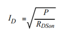
The RDS(on) is the on-state resistance of the MOSFET. The ID max can be calculated considering the RDS(on) at Tj(max). The graph in Figure 3 can be used to calculate the current for a specific temperature requirement.

After determining the theoretical maximum ID, the value must be validated by testing and verification. Other limiting factors will be considered and taken into account when finalizing and safeguarding the ID(max) provided in the datasheets. At Tj = 175°C, ID(max) = 495 A is regarded to be the theoretical capacity for PSMN70-40SSH. The ID(max) measurement is verified in laboratories where the junction temperature is ensured to be below Tj(max). The current will be limited by the thermal design of the PCB and the operating temperature.
The maximum capability of the device in a real-life application will depend on the mounting base (PCB) temperature, in the case of datasheet this is at 25°C and the calculated ID(max) is 495 A. The same principle can be used to calculate the application ID(max) for the relevant temperature. It is important to note that Tmb is likely to rise because of high current and MOSFET must operate below Tj(max) .
Limiting the MOSFET’s maximum junction temperature Tj to 175°C is driven by the reliability requirements that MOSFETs need to meet. And thus, 175°C is the temperature limit used by Nexperia for qualification and life test of MOSFETs in line with industry standards. All automotive power MOSFETs must meet the 175°C junction temperature specification.
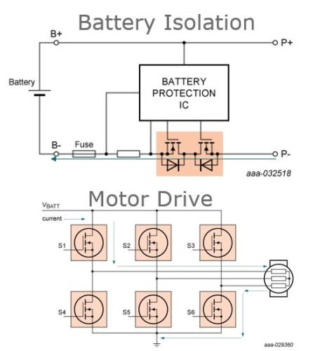
The ID current max capability becomes critical and most needed in the time between high system current occurring and the system reacting – the higher the capability the bigger the safety margins. In e-fuse/battery isolation, this is the time between an overcurrent situation’s detection and reaction; in motor drive applications, the time between rotor locks and the control system reacting becomes critical (Figure 4).
LFPAK package
MOSFET package structure, be it wire-bond or copper clip will affect how current will spread in the silicon die, along with package thermal all of which will impact ID(max) capability. Package design will also contribute to the overall performance of the MOSFET, its robustness and reliability all important characteristics.
For today’s high-power automotive and industrial applications with space constraints, Nexperia argued that the LFPAK comes with a smaller footprint and higher power density when compared with older wire-bond packages such as D2PAK. It delivers outstanding performance and high reliability.
The LFPAK copper clip technology not only contributes in MOSFETs achieving higher current capability, with its uniform current spread and low source inductance, it also helps MOSFETs handling the operation of such high current levels. Furthermore, the thermal mass of the copper clip minimizes the development of hotspots, resulting in better avalanche energy (EAS) and linear mode (SOA) performance.