As a material, GaN appears to have significant built-in advantages over silicon for many applications. There
During the last Nexperia Power live Event, many industry leaders discussed different topics related to gallium nitride technology. As a material, GaN appears to have significant built-in advantages over silicon for many applications. There are clearly many market applications that benefit from GaN, including power converters in the consumer, automotive, and space industries.
The GaN panel featured many industry leaders, including Caroline O’Brien, CEO of Kubos Semiconductor; Temoc Rodriguez, chief engineer at Ricardo; Mikael Björk, CEO of Hexagem; Dilder Chowdhury, director of strategic marketing at Nexperia, and Jim Honea, GaN applications director at Nexperia. Chowdhury is working mainly on medium to higher power in GaN, while Honea is a circuit designer for high-voltage applications.
Kubos Semiconductor is developing new technology and a new material called cubic GaN. “It’s the cubic form of gallium nitride and we can not only produce it on large-scale wafers — 150 mm and above — but potentially, they can scale to higher wafer sizes and can slot seamlessly into existing production lines,” said O’Brien.
Ricardo is working in the field of wide-bandgap (WBG) semiconductors to expand the electrification program with both silicon carbide and GaN. Rodriguez pointed out that Tesla was the first to employ SiC instead of IGBTs, and many companies are heading the same way with WBG solutions, including GaN, with the promise of increasing efficiency and reducing the size and weight of power converters.
Björk spoke about Hexagem’s development activities for high-quality GaN-on-silicon to reduce the cost and scale advantages of future applications. “We are looking at higher requirements in terms of voltage rating,” said Björk.
One of the wonderful things about new technologies like GaN, according to Nexperia, is that they make huge leaps in performance from generation to generation. All of the big victories in silicon have already been made; it’s all about incremental improvements at this stage in the technological life cycle.
Applications
Industry sectors ranging from automotive to telecommunications are being pushed to invest in more efficient power conversion and more electrification as societal pressure and regulation for lower CO2 emissions grows. Traditional Si-based power semiconductor technologies, such as insulated-gate bipolar transistors (IGBTs), have basic limitations in terms of operating frequency and speed, as well as poor high-temperature and low-current performance. The frequency and high-temperature performance of high-voltage Si FETs are similarly restricted. As a result, WBG semiconductors are becoming more popular in many applications.
“In applications markets, with improvements in terms of smaller design footprints, and because of the higher efficiencies, I think GaN enables applications that haven’t been recognized or widespread before, such as small base stations,” said O’Brien. “So I think there’s a real opportunity there for the smaller system design overall, and that opens up new and exciting opportunities to be developed.”

As Rodriguez pointed out, the key feature is the switching frequency response. It offers interesting applications up to 5–10 kW for DC/DC converters. “And that’s kind of a marker that can be considered in telecommunications and energy but also in consumer electronics,” he said. “There are plenty of applications centered on DC/DC converters to improve their efficiency and save energy.”
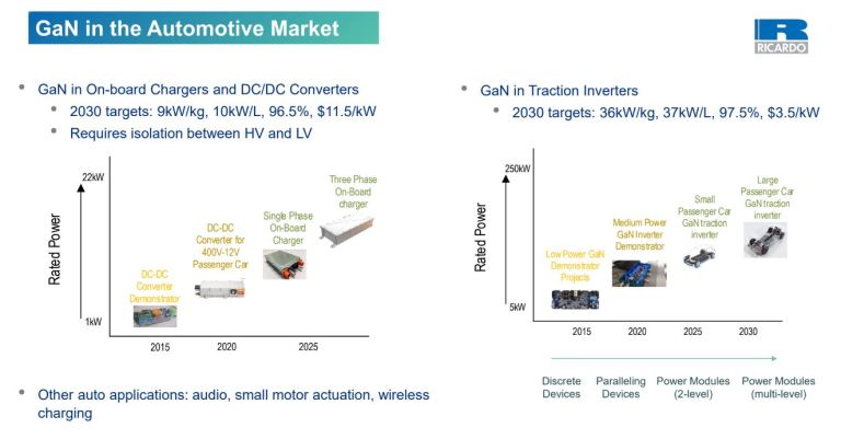
Rodriguez described the main applications of GaN in the automotive sector, as shown in Figure 2: “On the left side, you can see on-board chargers and DC/DC converters. At the moment, the on-board charger can reach 3.3 kW, maybe 7 kW, or moving toward 11 kW or 22 kW, stressing GaN. The current ratings aren’t compared with silicon carbide or IGBTs. That is limiting how much power you can use, and it’s also driving circuit designers to start looking at paralleling devices. So we’ve definitely started with DC/DC converters.
“We can easily imagine the first application being a 400-V to 12-V DC/DC converter,” he continued. “So this will be the one that takes power from your high-voltage battery and charges your 12-V battery and keeps it topped up. The next level will be to increase that power level to 5 kW. And the real challenge then becomes what to do when the automotive industry moves to an 800-V battery system.”
Björk highlighted the importance of the wafer and the fact that we are looking at higher and higher requirements in terms of voltages, as well as optimizing the production of GaN devices and getting a set of costs as low as possible. “Right now, 150-mm wafer is the market address, but in the future, you can scale up to 200-mm wafers, and who knows, there will probably be attempts at 300-mm wafers,” he said.
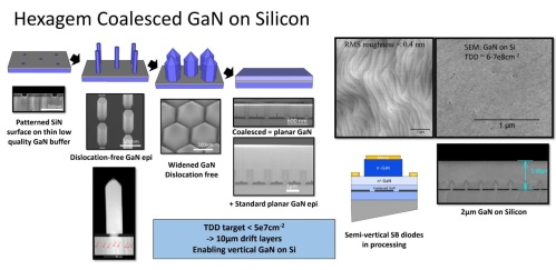
GaN-on-Si technology, the one most widely used, does not have a good reputation in terms of development. It has its challenges, and growing GaN-on-Si is not easy due to two main problems, according to Björk.
“Gallium nitride and silicon have very different lattice constants, so they don’t match,” he said. “So you have to grow fairly advanced stacks of different layers before you can put GaN on silicon, and when you do that, you create a lot of defects, dislocations that are detrimental, losses, and premature breakage. The other problem is a thermal expansion mismatch between GaN and silicon, so when you grow this to about 1,000˚C, when you cool down these two materials, they shrink at different rates and you can end up breaking the structure.”
Figure 3 shows the new technology developed by Hexagem on a very thin 100-nm silicon wafer. By modeling this surface, Björk said it is possible to grow defect-free GaN pillars. “A method has been developed to fuse these pillars into a planar layer,” he said. “We’re working on developing this process on other semiconductors.”
Honea emphasized the importance of the automotive industry. On-board chargers, DC/DC converters, traction inverters, and auxiliary inverters are all significant electrification opportunities for GaN. “The development of large batteries for electric vehicles is creating a lot of applications that no one imagined in the past,” Honea said.
Chowdhury said that, because of the low Qrr or virtual absence of the Qrr, this helps lower filter designs, resulting in much simpler designs. It greatly improves switching performance. GaN power transistors may be utilized in parallel with reasonable ease if the gate-driving circuitry is well-understood. Appropriate decoupling snubber circuit can help paralleling power GaN FETs easily. The most difficult problem is dealing with high voltages and switching frequencies, which many engineers may have never worked before with existing silicon technology.
GaN power semiconductors are gaining traction as a key component in the next generation of high-performance EVs, helping to reduce size and weight while increasing efficiency. These considerations address concerns with range. Engineers may use GaN to create power electronics systems that are 4× smaller and lighter and have 4× less energy loss than Si-based systems. Zero reverse recovery, which reduces switching loss in battery chargers and traction inverters, as well as higher frequency and quicker switching rates are among the benefits. Furthermore, decreased switching turn-on and turn-off losses can aid in the weight and volume reduction of capacitors, inductors, and transformers for applications such as EV chargers and inverters.
WBG technology is providing solutions as power-converter designers look for ways to improve efficiency and power density in their designs. GaN transistors are increasingly becoming the solution, but like their silicon counterparts, single devices still have upper limits to their current-handling capability. The use of such devices in parallel is a common approach. “One of the interesting things with GaN is that we can scale the size,” said Honea. “By putting GaN transistors in parallel, we can scale the power. However, if you put them in parallel, you multiply the resonances, and you have to make sure you don’t excite and amplify them.”
Design aspects
Rodriguez said that Ricardo has been working with SiC for many years with traction inverter solutions. Ricardo ran tests at GaN in this application area (Figure 4), putting two 30-kW applications on the same level. “From the simulations, you see a difference in peaks, as shown in Figure 4,” Rodriguez said. “I think the most eye-catching graphs here are those pie charts on how the losses are distributed, and that’s interesting because it shows that in silicon carbide, you can design the converter to have approximately equal switching and conduction losses. In this case, most of the losses are 63% switching losses and the rest are conduction losses, but in the gallium nitride inverter, things switch. In other words, the switching losses are almost eliminated, and you end up with a lot of conduction losses coming from multiple elements like bus bias and PCB.
“Now, of course, you may decide to parallel the device, increasing the cost, which will reduce your conduction loss without impacting your switching loss much,” he added. “While you can’t do that with silicon carbide, the switching losses are there and get worse by parallelizing the devices. So this is a key point for gallium nitride and why I think it will be the technology to dominate in the near future.”

Switching losses are also significantly reduced when GaN is used. The losses that occur during this transition are minimized by increasing the speed at which the switch is turned on utilizing GaN technology. By increasing the switching frequency, many big components shrink in size (such as the transformer, inductors, and output capacitors). In comparison with silicon, GaN has a greater thermal conductivity and can endure higher temperatures. Both contribute to a reduction in the requirement for thermal management components such as bulky heatsinks and cooling, resulting in considerable power supply size and weight savings.
Supply chain
The capability to concurrently design the product and the supply chain is becoming a key competence in manufacturing companies. “One of the biggest advantages of GaN-on-Si is that it is grown on silicon substrates, so it’s 150 mm right now, and it’s being worked on to go to 200 mm, and most reactors currently accommodate both,” said Chowdhury. “From that context, actually increasing the number of reactors can increase the initial supply material for the fab. There are numerous silicon fabs located throughout the world, and it’s much easier to increase capacity within existing silicon fabs. And for the back end at the die level or at the packaging level, we have got a vertical organization, where we have got our own packaging in multiple sites in far east and around the globe. This allows us to have volume production, especially for packaged devices. At die level, obviously, we are investing quite a lot to increase the capacity and meet the demand. So I hope this gives an initial understanding of the supply-chain challenges that we are trying to handle.”
According to O’Brien, the industry must start preparing, whether it’s vertically integrated supply chains, pure foundries, or compound semiconductors. Demand for components is rising in nearly every industry at the same time, particularly in the automotive, smartphone, medical, and industrial sectors, which require an increasing number of components for finished goods. Sudden changes in the competitive climate can put a burden on supply and distribution chains, creating problems with logistics and lead times, as well as slowdowns due to crucial supplier closures or production stoppages.